
It’s all about the monetizing of the Xeon.” – Dan McNamara, Intel PSG
Intel’s Data-Centric Innovation Summit, held earlier this month at Intel’s Santa Clara HQ, incorporated a lot of talk about the role of Intel’s FPGA products in the “great scheme of things.” Last week, I discussed the FPGA market with $8 billion in annual sales that Intel’s targeting—see “The New, New Intel Unleashes a Technology Barrage”—but that’s hardly the full story for Intel’s FPGAs. Dan McNamara, Senior VP and General Manager of Intel’s PSG (Programmable Systems Group), had a couple of opportunities to tell more of that story and to provide his carefully nuanced description of Altera’s transformation into Intel’s Programmable Systems Group. One opportunity was a lunchtime discussion at a catered affair in a walled-off section of Intel’s cafeteria, and the other was his formal afternoon presentation. Let’s take the two opportunities in reverse order, because the later presentation actually sets the stage for McNamara’s briefer, more off-the-cuff remarks at lunch.
In his afternoon presentation, McNamara said that he thinks of FPGAs as a “data shovel.” OK, not a very glamorous marketing analogy but an efficient, two-word description if that’s what you’re looking for. FPGAs remove data bottlenecks and accelerate the work, he said. I guess that’s what a shovel does, if you use the right tongue angle, as YouTube video star Dave Jones might say.
Then McNamara further parsed his meaning. “The cloud’s always looking to provide more services while managing TCO,” he explained.
Translation: Wherever possible, we want to offload more mundane tasks from our incredibly expensive Xeon server processors and move them to lower-cost, more efficient processing engines to make room in the Xeon for tasks that deliver more revenue to data center operators and more value to data center customers. In many cases, those offload engines are constructed in hardware using programmable logic—aka FPGAs.
Quick aside to lunch where McNamara gave a more succinct explanation:
“It’s all about the monetizing of the Xeon.”
This is the reason Intel’s currently giving for its acquisition of Altera. (For more details about the acquisition back in 2015, see Kevin Morris’s “After Intel and Altera: What Happens to FPGA?”). Is monetizing the Xeon a good reason to buy an entire FPGA company? Well, sure it is. Earlier in the day, during the Data-Centric Innovation Summit, Intel’s EVP and GM of the Data Center Group Naveen Shenoy had said that Intel had shipped 220 million Xeon processors worth an aggregate value of $130 billion over the last 20 years. (Intel is celebrating the Xeon processor’s 20th birthday this year.)
Here’s a Xeon family tree, for those keeping score:
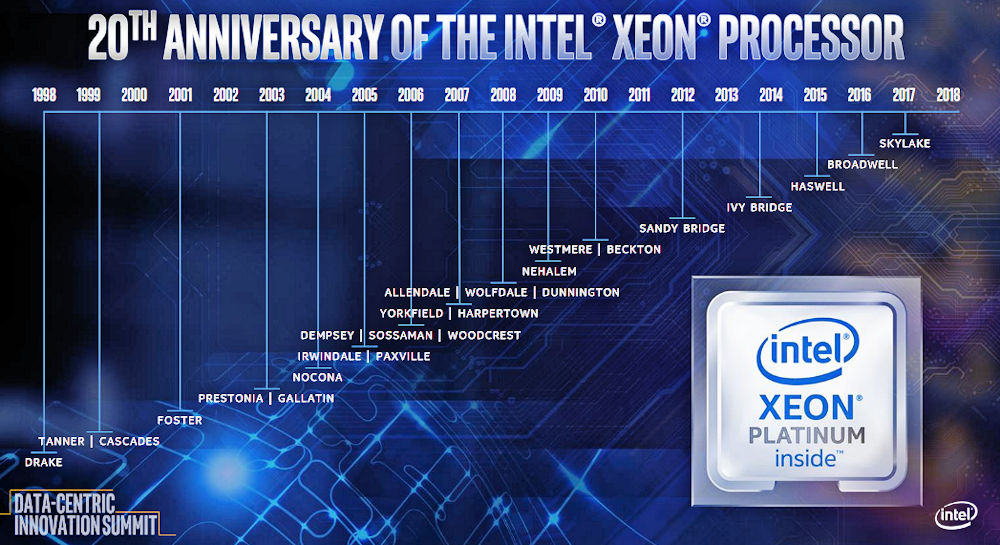
Figure 1: The Intel Xeon family tree spans two decades. (Image source: Intel)
During his morning talk, Shenoy made it crystal clear that Intel was not about to move high-value tasks from the very, very profitable Xeon processor line to the still-pretty-darn-profitable Intel FPGA product line. He did that by citing the new features coming up in future Xeon processor designs that will make Xeon processors more valuable to data centers, including built-in support for Intel’s Optane DC Persistent Memory DIMMs, a new layer in the ever-expanding memory hierarchy, new instructions for AI and machine learning dubbed “Intel Deep Learning Boost (DLBoost),” and support for a new AI-oriented, 16-bit, floating-point data type originally developed by Google called BFloat16, which is useful for neural-network training rather than inference.
Support for Optane DC persistent memory and the initial version of DLBoost are scheduled to appear later this year in a 14nm Xeon iteration code named Cascade Lake. The follow-on Cooper Lake version of Xeon, also fabricated with 14nm process technology, will appear in 2019 with an improved, second-generation version of the DLBoost extensions and BFloat16 support. By 2020, Intel intends to roll these innovations and more into a 10nm device called Ice Lake. Shenoy didn’t elaborate on the “more” part of that last sentence.
Segue back to FPGAs and Dan McNamara’s afternoon talk, where he discussed several tasks ripe for Xeon offloading, including “lookaside acceleration” such as neural network inferencing, image and video transcoding, and database searching; network infrastructure acceleration including network packet processing, storage, and security; and enterprise application acceleration including data analytics, financial processing, video processing, network and data security, and genomics. These target applications are a sure bet for Intel PSG’s FPGAs, because they’re already being performed by an increasing number of Intel and non-Intel FPGA boards plugged into servers located in data centers around the world.
Getting down to the brass tacks of production and product delivery, McNamara said that Intel PSG’s 14nm FPGA products are in production and that his group was now focused on “filling out the family.” (Translation: Intel PSG is busy designing more 14nm parts and bringing them into production.) McNamara also said that, going forward, the 14nm devices would be the dominant design-win vehicle for his group, and he mentioned that we will see more use of Intel’s EMIB (Embedded Multi-die Interconnect Bridge)—a form of 2.5D chip assembly—in future Intel PSG products to add functions such as embedded ARM cores and high-speed SerDes transceivers.
McNamara said that his group is going “full steam ahead” on 10nm FPGA designs and that Intel planned to sample these new parts next year. You might want to take that statement with a grain of salt when you consider that the 10nm Ice Lake Xeon variant discussed a couple of paragraphs above isn’t scheduled to ship until 2020. My spider sense and the usual Intel financial boiler plate caution about future predictions—“forward-looking statements… involve a number of risks and uncertainties”—tell me not to take that sampling schedule to the bank. As Shenoy said earlier in the day during a Q&A session, “I don’t talk to customers about nm.”
There’s a valid reason for that in Intel’s recent history, and I don’t see 10nm FPGAs upstaging Intel’s flagship 10nm Xeon processors or even getting in the flagship’s way within the 10nm fab. Even with all of the transition talk during the Data-Centric Innovation Summit about Intel’s migration from processor-centric to data-centric, I don’t see processors taking a back seat to FPGAs in Intel’s most bleeding-edge process technology. That’s not to say it couldn’t happen; however, remember McNamara’s lunch statement: it’s all about monetizing Xeon.
Finally, McNamara discussed Intel’s recent acquisition of eASIC in the context of Intel PSG and FPGAs. During his afternoon talk, he said, “eASIC adds an end-to-end lifecycle solution” through its structured ASICs, which have a lower NRE than ASICs. Adding eASIC to the portfolio means that Intel will supposedly have a way to reduce the cost of FPGA-based designs by taking these designs and rolling them into eASIC’s structured ASICs, which will have lower unit costs and lower power consumption than the FPGAs they replace. Here’s the relevant slide from McNamara’s talk:
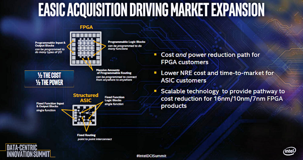
Figure 2: Intel’s justification for its acquisition of eASIC includes synergy with Intel PSG’s FPGAs (Image source: Intel)
Earlier, during lunch, McNamara said, “Look at eASIC as a little bit of a hedge.” Tasks that aren’t changing twenty times a month are ripe for conversion to a structured ASIC.
This is the existing eASIC story, so it can certainly work for Intel. However, if you’d like a deeper analysis of Intel’s eASIC acquisition, be sure to read Kevin Morris’s July 17 article titled “Intel Acquires eASIC – Why?”
Leave a Reply
You must be logged in to post a comment.